Expert Speak | 10 April, 2026
Beyond ASML: Towards Middle Power Semiconductor Sovereignty
Spotlight
- ASML’s EUV monopoly creates a critical chokepoint in the global semiconductor supply chain.
- China’s progress toward a domestic EUV prototype demonstrates that export controls can accelerate self-reliance rather than prevent it.
- Japan’s materials, Korea’s manufacturing, UAE’s capital, and India’s talent form a viable four-pillar path to semiconductor sovereignty.
Artificial Intelligence (AI) has emerged as the defining technology of the 21st century. Many attribute advanced progress in AI to algorithms, large datasets, and software innovation, which often obscures a fundamental reality: AI capabilities rest heavily on physical hardware.
This foundation relies on advanced semiconductors, chips with the high computational power and energy efficiency required to train and run frontier AI models. The number of transistors packed onto a chip determines its computational power. A critical process in chip manufacturing is lithography, process in which light is used to etch circuit patterns onto silicon.
Lithography for the Layman
Lithography is the process by which intricate circuit designs are etched onto a silicon wafer using light. These circuits comprise of transistors that power modern chips. While the chip itself can be seen through the naked eye, the circuits printed on it are measured in nanometres.
Producing a computer chip requires printing minute circuit patterns onto silicon wafers using machines known as lithography scanners. However, the process depends on an ecosystem of supporting materials including specialised chemicals, stencils, protective films, as well as complementary processes such as design software, water purification and air filtration systems. For middle-power countries, these supporting components (the chemicals, stencils, protective films, software, and purification systems) represents the most realistic entry points into the chip supply chain, rather than attempting to manufacture the scanners themselves.
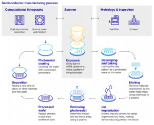
Source: FabricatedKnowledge
For years, the industry relied on Deep Ultraviolet (DUV) lithography as the primary technique for chip fabrication. As device scaling approached the 7‑nanometer technology node, the DUV process encountered functional limitations. To continue manufacturing advanced chips, manufacturers were forced to adopt “multiple patterning,” a method in which the same layer is printed several times to achieve the required resolution. While effective, this approach substantially increased production costs and time, as well as heightened the probability of defects.
The introduction of Extreme Ultraviolet (EUV) lithography marked a significant advancement in semiconductor manufacturing. This technology uses light with a wavelength of just 13.5 nm, enabling it to reliably print features smaller than 7nm in a single exposure. As a result, a greater number of transistors can be integrated onto a chip, thereby enhancing computational performance and improving energy efficiency.
ASML: The Hidden Giant Behind the Semiconductor Industry
ASML is currently the sole supplier of Extreme Ultraviolet (EUV) lithography systems globally.
ASML functions as a de facto gatekeeper to the advancement of semiconductor technology, as EUV represents the only scalable approach for mass production of advanced chipsets required to support contemporary AI applications.
This near-total monopoly positions ASML as a critical chokepoint within the global semiconductor supply chain. Consequently, its strategic decisions extend beyond considerations of profitability and encompass broader implications for international security. Since the same chips that power a chatbot also power an autonomous drone or a nuclear simulation, these machines are classified as “dual-use” technology. This elevates ASML from a successful Dutch company to a national security asset.
While the United States (US) designs the world’s most advanced chips (via companies like NVIDIA) and Taiwan manufactures them (via TSMC), both processes remain dependent on ASML’s lithography systems . Since ASML is a foreign entity, the US government cannot regulate its operations directly and must rely on a partnership with the Dutch government. This transforms the Netherlands from a traditional trade partner into a strategic actor within the global semiconductor ecosystem.
In addition to its diplomatic significance, ASML acts as a domestic economic engine by generating €28.3 billion in net sales in 2024. Recognising the company’s strategic importance, the Dutch government recently initiated “Project Beethoven,” a €2.51 billion investment plan in infrastructure and education designed specifically to prevent ASML from expanding operations abroad amid concerns over local immigration and tax policies.
Since ASML’s machines rely on critical components and intellectual property originating in the US, Washington holds a “regulatory veto” over Dutch exports. This authority was exercised when the US applied diplomatic pressure on the Dutch government to effectively block EUV machine sales to China, creating a firm barrier to the hardware required for producing cutting-edge chips.
In response, China intensified efforts toward technological self-reliance, utilising state subsidies, prioritising research and development, and implementing domestic-first policies to reduce reliance on foreign suppliers and accelerate technological autonomy. These measures appear to be producing results. In December 2025, Reuters reported that China developed a domestic EUV prototype, marking a breakthrough in a domain previously considered inaccessible. Although not yet commercially viable, the achievement suggests that sustained pressure may accelerate indigenous innovation rather than prevent it.
Proposing Middle Power Partnership: A Four-Pillar Ecosystem
China’s experience offers two critical takeaways: first, there is a severe chokepoint in the semiconductor supply chain, second, sustained investment can provide a means of bypassing it.
For middle powers like Japan, South Korea, the United Arab Emirates, and India, the major lesson is that relying on a single, controlled supply chain is a strategic vulnerability.
At the same time, these states occupy a comparatively more favourable position within the existing export control framework than China, though each faces its own distinct trade pressures and limitations on technology access . Individually, these states are already pursuing ambitious industrial strategies to strengthen domestic semiconductor capabilities.
Friend-Shoring the Lithography Ecosystem
Individually, these states encounter significant shortcomings if they attempt to build autonomous, start-to-finish supply chains capable of rivaling ASML. However, it is possible for nations to coordinate a practical, and resilient supply network that breaks the existing monopoly and establishes a viable, alternative pathway for producing a competing EUV scanner and the advanced chips it prints.
Japan provides the physical link in this supply chain. It brings indispensable chemical expertise and EUV-grade materials that act as a barrier to entry for other nations. Firms such as JSR, Shin-Etsu Chemical, and Tokyo Ohka Kogyo collectively dominate photoresist supply—inputs without which no lithography system can function. They provide the foundational hardware components that make lithography physically possible.
Korea can serve as the partnership’s high-volume testing ground. It offers the fabrication scale and cleanrooms necessary to take an EUV prototype and scale into a commercial-grade manufacturing tool, and is already a major player in the High Bandwidth Memory sector. Korea possesses the capacity to turn blueprints into physical, mass-produced silicon.
The UAE anchors the coalition economically rather than technically: sovereign wealth capital from government setup firms such as MGX, a technology investment company can absorb the front-loaded investment risk that private markets will not take on for a decade-long hardware program. At the same time, the country’s rapidly expanding AI computing infrastructure; exemplified by the Stargate UAE data center, creates the massive domestic demand needed to sustain long-term semiconductor production.
India can provide a vast engineering talent pool, already comprising 20 percent of the global semiconductor design workforce. When channelled through a joint coalition design center, this talent represents a scalable resource for iterating EUV system architecture under shared IP terms. Additionally, the partnership benefits from immense commercial scale, as the government projects that domestic semiconductor demand will reach US$110 billion by 2030. Notably, ASML itself is now actively seeking Indian partners — validating India’s readiness to move from talent exporter to strategic node within the global semiconductor ecosystem.
Conclusion
The semiconductor supply chain is the backbone of 21st-century strategic power. As AI reshapes economies, militaries, and societies, the nations that control the hardware pipeline will shape the rules of the emerging order. At present, that pipeline runs through a single bottleneck in Veldhoven, Netherlands. For middle powers, the choice is to either accept permanent dependency on a supply chain governed by the strategic priorities of others, or invest collectively in an alternative. The four-pillar partnership proposed here is not a call to replicate ASML overnight—it is a call to assemble, across four nations, the capabilities that ASML currently concentrates within one company.
Japan’s materials, Korea’s manufacturing capacity, the UAE’s capital, and India’s engineering talent are, individually, impressive national assets. Together, they constitute something far more consequential: a credible path toward technological self-determination.
The window to act is narrowing—every generation of chips that passes without an alternative deepens the dependency.
Sovereignty in the age of AI is measured not in rhetoric, but in nanometres. The question these nations must answer is not whether they can afford to pursue this partnership, but whether they can afford not to.
Siddharth Yadav is a Fellow, Emerging Technologies, ORF Middle East.
Khush Advani is Research Assistant, Development Studies, ORF