
 Global
Expert Speak | 25 August, 2026
Power Up: How Spintronic Nanodevices Can Fuel the Future
The following excerpt is from Chapter 6 — ORF Global Quarterly | Energy and Tech: Powering the Future.
The exponential growth of Artificial Intelligence (AI) computing is pushing conventional charge-based electronics towards their fundamental limits in power consumption and scalability. As transistors shrink and processing demands increase, the heat generated by leakage currents and switching energy is exceeding what chip architectures can safely dissipate. This has drawn attention to spintronics,[1] a branch of nanotechnology that exploits both the magnetic and electrical properties of electrons. Spintronic nanodevices offer superior energy efficiency for brain-inspired computing architectures, with magnetic tunnel junctions emerging as especially promising building blocks that are compatible with existing chip manufacturing processes.[2]
The technology is now considered not only a key enabler of next-generation, low-power AI hardware but also a foundation for next-generation memory, logic, and quantum computing. With applications already spanning the automotive, aerospace, and data-centre sectors, spintronics has become a strategic priority for countries with the manufacturing capacity to compete for it, driving targeted R&D funding, national roadmaps, and industry partnerships aimed at securing technological leadership and supply chain resilience. This strategic importance is already reshaping geopolitics and driving indigenisation. For the Global South, which sits almost entirely on the consumer side of this value chain, the stakes are high. The technology’s concentration among a handful of advanced economies risks blocking the entry points for the Global South to be a part of the next wave of technological change.
The Historical Arc
The origins of spintronics can be traced to the Stern–Gerlach experiment of 1922 in Germany, which provided the first experimental evidence that electrons possess an intrinsic quantum property known as ‘spin’.[3] This concept was formally theorised in 1925 by Dutch-American physicists George Uhlenbeck and Samuel Goudsmit, whose work laid the foundation for decades of scientific enquiry.[4] The technological significance of electron spin, however, was not realised until 1988, when the physicists Albert Fert of France and Peter Grünberg of Germany discovered that the spin orientation of electrons could dramatically influence the flow of electrical current through ultra-thin metallic layers. This phenomenon, known as Giant Magnetoresistance (GMR),[5] enabled the development of sensors and memory devices capable of storing and retrieving information by detecting electron spin states rather than relying solely on electrical charge.
For the Global South, which sits almost entirely on the consumer side of the nanotech value chain, the stakes are high.
Commercialisation followed in 1997, when IBM first deployed spintronic technology in hard disk drives (HDDs).[6] Subsequent advances during the 2000s increased HDD storage capacity by roughly two orders of magnitude within a decade. The second wave of commercial adoption emerged with the transition to Magnetoresistive Random-Access Memory (MRAM) in the latter half of the 2010s. Milestones such as GlobalFoundries’ introduction of STT-MRAMn in 2016 and TSMC’s 22nm Ultra-Low Power process in 2017 significantly expanded the technology’s applications across the automotive and Internet of Things (IoT) sectors.[7]
Figure 1: The Evolution of Spintronics

Source: Authors’ own, generated using Sonnet 4.6[8]
The Technology and its Applications Today
Spintronics is gaining cross-sectoral significance because its advantages are most evident where conventional electronics encounter fundamental physical limits. In AI hardware, the technology addresses two principal constraints on continued scaling: energy consumption and memory bandwidth. Global data-centre electricity consumption reached approximately 415 TWh in 2024, representing roughly 1.5 percent of worldwide electricity use, and is projected to more than double to 945 TWh by 2030.[9] Spintronic chips enable compute-in-memory architectures that eliminate the energy cost associated with moving data between processors and memory. They are already deployed in edge AI applications, powering devices such as industrial sensors and smart cameras.[10]
In the automotive sector, magnetoresistive random-access memory (MRAM) is now in volume production for microcontrollers used in electric vehicles. These chips capture realtime engine control data, facilitating functions including advanced driver assistance systems, reliable over-the-air firmware updates, and infotainment systems. In aerospace and defence, radiation-hardened MRAM is being deployed in satellites, spacecraft, and military electronic platforms, where conventional flash memory is susceptible to degradation from cosmic radiation.[11]
Spintronic magnetic sensors are also demonstrating utility in biomedical applications, including disease diagnosis, medical imaging, and detection of biomagnetic fields, owing to their high sensitivity and robustness.[12] In industrial automation and the IoT, spintronic sensors and embedded MRAM are increasingly employed in programmable logic controllers, robotic systems, and connected manufacturing devices. The non-volatility of MRAM allows factory systems to recover instantaneously after power interruptions without data loss, offering a reliability advantage over flash-based alternatives in continuous production environments.[13]
Beyond these established applications, spintronics is expected to play key roles in quantum computing, navigation, and advanced communication systems. Its relevance to defence and security has elevated the technology to a matter of strategic state interest. More broadly, the semiconductor industry has become a central arena of global technological competition, with its importance extending beyond economic value to encompass national security and technological sovereignty. This has prompted a worldwide shift from market-led to security-driven policy approaches. Countries across the world have taken diverse approaches to spintronics, choosing various applications that drive their economies and future strategies. The United States, which led the spintronics market in North America in 2024, made advancements in aerospace and defence applications.[14]
Among countries of the European Union, France has taken a leading role in the domain, having invested about €38 million over eight years in the PEPR SPIN national research programme targeting applications in AI, cloud storage, and the communication networks of the future.[15] Meanwhile, Chinese initiatives funding domestic research and development in spin, as well as its broader focus on quantum technology and semiconductors, has driven breakthroughs in spintronics.[16] Mastery of spin-based memory is expected to soon become inseparable from broader objectives of digital sovereignty, AI leadership, and defence preparedness in an era of intensifying technological competition.
Figure 2: Neuromorphic Spintronics Market Projections by Application (2023–2033) and Application Share by End Use (2024)
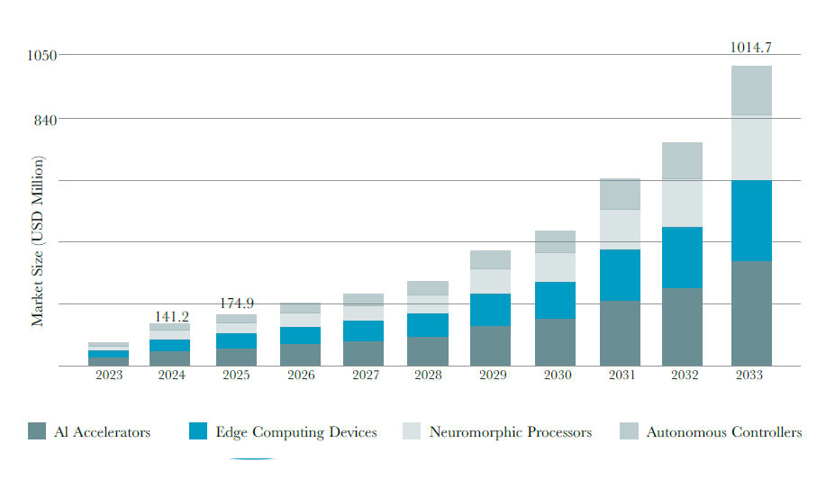
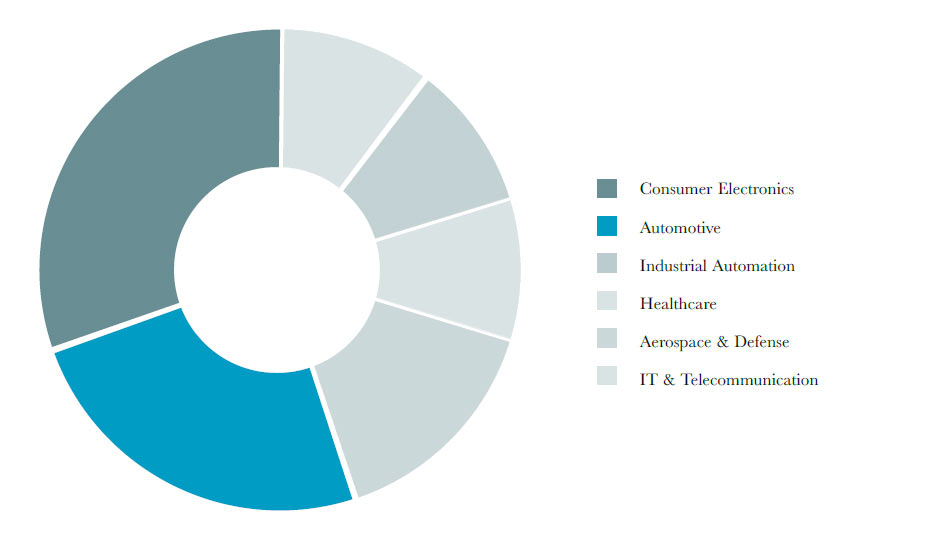
Source: Grand View Research[17]
The Concentration
As advanced industrial economies compete to dominate this technological frontier, spintronics also carries important implications for countries that remain outside the manufacturing race. The global spintronics market is highly concentrated. In 2025, the Asia-Pacific accounted for 48.4 percent or US$0.7 billion of the US$1.44 billion global market, driven almost entirely by the semiconductor manufacturing hubs of South Korea, Japan, Taiwan, and China.[18] North America, led by the US, represents US$0.31 billion, attributable to its strong technological infrastructure, investment in scientific research, and existing industrial base.[19] Meanwhile, South America’s share is just US$0.06 billion, and the Middle East and Africa, taken together, account for US$0.09 billion;[20] these figures are marginal relative to the technology’s strategic importance.
The barriers to entry are substantial. Fabricating advanced semiconductor nodes requires multi-billion-dollar investments and highly specialised technical expertise. As a result, most Global South nations remain confined to the consumer end of the value chain, purchasing chips, controllers, and IoT devices designed and manufactured elsewhere. High production costs and integration challenges already constrain 27 percent of potential market applications globally.[21] These obstacles are compounded by energy and infrastructure deficits, limited research ecosystems, and the persistent outflow of skilled talent.[22] Without deliberate intervention, the spintronics transition risks deepening the digital divide by reinforcing existing patterns of technological dependence and exclusion.
The Opportunity Window
MRAM holds particular potential for the Global South due to its reduced power usage combined with high speed and endurance.[23] This is highly advantageous for energyconstrained environments like sub-Saharan Africa and South Asia, where edge computing is most needed for research and applications but power supply is least reliable. Similar to mobile banking’s bypass of standard banking infrastructure to enable financial inclusion,[24] MRAM-powered edge devices could allow these economies to participate in this revolution without the infrastructure assumptions of more developed environments like continuous power.
Despite the barriers to entry, China’s experience demonstrates that participation in the spintronics market is achievable. The country’s Ministry of Science and Technology has made the expansion of the memory industry a pillar of its semiconductor indigenisation strategy.[25] In late 2025, Shanghai Siproin Microelectronics began commercial shipments of China’s first STT-MRAM chips, marking the country’s first commercially available emerging memory technology.[26] This demonstrates that sustained state support, long-term investment, and a willingness to absorb extended development timelines can help narrow technological gaps.
India’s semiconductor push and Brazil’s deep-tech clusters in São Paulo and the broader Latin American materials-science ecosystem similarly represent potential entry points at the research and design layer, even if advanced fab-level participation remains distant. For smaller economies, the more immediate path is through procurement policy for MRAM, which over time could lead to design and integration capability.
The Geopolitics of Spin
State-level strategic interest has made spintronics part of the broader contest for technological sovereignty. This is especially evident in the US-China semiconductor rivalry, where escalating and retaliatory export controls have shaken the sector and begun to reshape which countries can access, and which must indigenise, the next generation of memory technology. Under the current US regulations, MRAM is not included in the controlled categories. As the calculus shifts, this cannot be taken for granted.
For China, export controls have functioned as an accelerant for domestic ambition. Siproin’s achievement, combined with other Chinese manufacturers such as ChangXin Memory Technologies’ DDR5 DRAM—the current-generation standard for the volatile, high-speed memory used in computers and smartphones—and Yangtze Memory Technologies Corporation’s NAND—the flash storage technology underlying solid-state drives and mobile devices—forms an increasingly complete domestic memory ecosystem.[27]
Meanwhile, the European Union’s Chips Act has aligned with the US chokepoint strategy, and the industry is actively advancing nextgeneration MRAM.[28] The net effect is a technology landscape in which the memory supply chain is dividing along geopolitical lines.
Future Trajectories
The future spintronics landscape will be shaped by several factors. The expansion of AI computing is likely to be the strongest driver of growth, with edge AI emerging as a major market for MRAM. Tighter US export controls could provide a further boost, particularly for China’s domestic ecosystem. As the Siproin breakthrough illustrates, restricting access to foundry services creates the industrial policy rationale for domestic capability development. The primary risk of slowdown is process economics. If silicon CMOS scaling proves more durable than expected, the speed of the MRAM transition could decrease. A recalibration in US-China technology relations could similarly reduce the pressure driving Chinese indigenisation.
What is clear is that the decisions made in 2026—including which architectures to fund and regulate and which countries to include in the emerging memory ecosystem—will shape the spintronics landscape to come. For the Global South, the window to participate in those decisions is open but narrowing. Spintronics may not define the next few years, but these years will do much to define who benefits from spin.
Amoha Basrur is Junior Fellow, Centre for Security, Strategy and Technology (CSST), ORF.
Pranoy Jainendran is Research Assistant, CSST, ORF.
The authors acknowledge that Sonnet 4.6 was used to generate Figure 1 and for refining language for clarity.
[1] Nanotechnology is the understanding and control of matter at the nanoscale, at dimensions between approximately 1 and 100 nanometres, where unique phenomena enable novel applications.
[2] Julie Grollier et al., “Neuromorphic Spintronics,” Nature Electronics 3 (2020):360, https://doi.org/10.1038/s41928-019- 0360-9.
[3] Horst Schmidt-Böcking et al., “The Stern-Gerlach Experiment Revisited,” The European Physical Journal H 41 (2016): 327, https://doi.org/10.1140/epjh/e2016-70053-2.
[4] George E. Uhlenbeck and Samuel A. Goudsmit, “Spinning Electrons and the Structure of Spectra,” Nature 117 (1926): 264, https://doi.org/10.1038/117264a0.
[5] Vincent Cross et al., “The 2007 Nobel Prize in Physics: Albert Fert and Peter Grünberg,” in: The Spin. Poincaré Seminar 2007 (Progress in Mathematical Physics, Vol. 55) ed. Bertrand Duplantier, Jean-Michel Raimond, and Vincent Rivasseau (Birkhäuser, 2009), 147-6, https://doi.org/10.1007/978-3-7643-8799-0_5.
[6] “1990: Magnetoresistive Read-head HDD Introduced MR, GMR & TMR Heads Deliver Successive Increases in Storage Density,” Computer History Museum, https://www.computerhistory.org/storageengine/magnetoresistive-read-headhdd- introduced/.
[7] “GLOBALFOUNDRIES Launches Embedded MRAM on 22FDX® Platform,” Everspin Technologies, September 15, 2016, https://www.everspin.com/news/globalfoundries-launches-embedded-mram-22fdx%C2%AE-platform; TMSC, 2017 Annual Report, April 19, 2018, investor.tsmc.com/sites/ir/annual-report/2017/e_11_3.pdf.
[8] Otto Stern and Walther Gerlach, “Der experimentelle Nachweis der Richtungsquantelung im Magnetfeld,” Zeitschrift für Physik 9(1922): 1, https://link.springer.com/chapter/10.1007/978-3-540-70626-7_214; Priti Rajput et al., “A Review on—Spintronics an Emerging Technology,” Silicon 14 (2022), https://link.springer.com/article/10.1007/s12633-021- 01643-x; “Spintronics Market to Witness 36.48% CAGR Amid Surge in AI, IoT, and Electric Vehicles,” Precedence Research, Januray 28, 2026, https://www.globenewswire.com/news-release/2026/01/28/3227739/0/en/Spintronics- Market-to-Witness-36-48-CAGR-Amid-Surge-in-AI-IoT-and-Electric-Vehicles.html.
[9] “Energy and AI,” International Energy Agency, April 10, 2025, https://www.iea.org/reports/energy-and-ai.
[10] Ibrahim A. Tasiu et al., “Spintronics Technology: A Comprehensive Review of Materials, Applications, and Future Trends,” Journal of Science: Advanced Materials and Devices 11 (2026): 101086, https://doi.org/10.1016/j.jsamd.2025.101087; “Exploring Spintronic Devices in Nanotechnology Applications,” Eureka by patsnap, October 21, 2025, https://eureka. patsnap.com/report-exploring-spintronic-devices-in-nanotechnology-applications.
[11] “Introducing Enhanced MRAM Product Family for Space and Defense,” Avalanche Technology, July 29, 2024, https://www. avalanche-technology.com/avalanche-technology-introduces-enhanced-mram-product-family-for-space-and-defense/.
[12] Shahriar Mostufa et al., “Spintronic Devices for Biomedical Applications,” npj Spintronics 2 (2024): 26, https://doi. org/10.1038/s44306-024-00031-6.
[13] “Case Study: Koyo Electronics Industries Programmable Logic Controller (PLC),” Everspin, 2015, https://www.everspin. com/factory-automation.
[14] Grand View Research, Neuromorphic Spintronics Market (2025 – 2033), 2025, https://www.grandviewresearch.com/industryanalysis/ neuromorphic-spintronics-market-report.
[15] “France 2030: The CEA and CNRS are Leading a National Spintronics Programme for Frugal, Agile, and Sustainable Digital Technology,” CNRS, January 29, 2024, https://www.cnrs.fr/en/press/france-2030-cea-and-cnrs-are-leadingnational- spintronics-programme-frugal-agile-and.
[16] “China to Include Quantum Technology in its 14th Five-Year Plan,” The State Council, The People’s Republic of China, October 22, 2022, https://english.www.gov.cn/news/videos/202010/22/content_WS5f90e700c6d0f7257693e3fe.html; “Chinese Scientists Make Breakthrough in the Field-Free Full Switching of Chiral Antiferromagnetic Order,” National Natural Science Foundation of China, https://www.nsfc.gov.cn/english/site_1/news/A2/2026/04-13/522.html; Ke Meng et al., “Room- Temperature Organic Spintronic Devices with Wide Range Magnetocurrent Tuning and Multifunctionality via Electro- Optical Compensation Strategy,” Advanced Materials 37 (2025):11, https://doi.org/10.1002/adma.20241799Fig15.
[17] “Neuromorphic Spintronics Market (2025 – 2033)”.
[18] “Spintronics Market, May 2026,” Fortune Business Insights, 2026, https://www.fortunebusinessinsights.com/spintronicsmarket- 110877.
[19] Spintronics Market, May 2026, https://www.fortunebusinessinsights.com/spintronics-market-110877.
[20] Spintronics Market, May 2026, https://www.fortunebusinessinsights.com/spintronics-market-110877.
[21] “Spintronics Market, May 2026,” Business Research Insights, 2026, https://www.businessresearchinsights.com/marketreports/ spintronics-market-111846.
[22] World Bank, Forging Viet Nam’s Semiconductor Future: Talent and Innovation Leading the Way, September 2025, Washington DC, World Bank Group, 2025, https://openknowledge.worldbank.org/server/api/core/bitstreams/fdbcbbbf-84e9-4edbb1ff- b7caa4c86bcb/content.
[23] Shanon Davis, “The 2025 MRAM Global Innovation Forum to Showcase MRAM Technology Innovations, Advances, & Research from Industry Experts,” Semiconductor Digest, December 8, 2025, https://www.semiconductor-digest.com/ the-2025-mram-global-innovation-forum-to-showcase-mram-technology-innovations-advances-research-from-industryexperts.
[24] ITU Telecommunication Standardization Sector, The Mobile Money Revolution Part 2: Financial Inclusion Enabler, May 2013, Geneva, International Telecommunication Union, https://www.itu.int/dms_pub/itu-t/oth/23/01/ t23010000200002pdfe.pdf.
[25] Yole Group, “China’s Next Move: the Five-Year Plan that Could Reshape Semiconductors,” Yole Group, December 1, 2025, https://www.yolegroup.com/strategy-insights/chinas-next-move-the-five-year-plan-that-couldreshape- semiconductors.
[26] “TechInsights Confirms China’s First Commercial STT-MRAM Chips,” TechInsights, December 8, 2025, https://www. techinsights.com/blog/techinsights-confirms-chinas-first-commercial-stt-mram-chips.
[27] “TechInsights Confirms China’s First Commercial STT-MRAM Chips”.
[28] “Bringing SOT-MRAM Technology Closer to Last-level Cache Memory Specifications,” imec, December 16, 2024, https://www.imec-int.com/en/articles/bringing-sot-mram-technology-closer-last-level-cache-memory-specifications.